

Let’s go through a brief description of all the steps involved in the process of PCB designing Part -2
2. Preparing the Design:

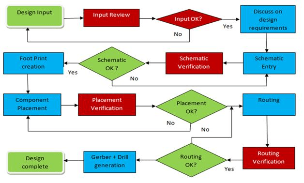
Schematic capture:
The first thing involved in preparing the design is its schematic circuit capture. For that purpose, you need to enter the circuits into a schematic editor, place the electrical components in the schematic and establish the net connections.
Netlist:
Once you’ve completed the schematic capture, you move on to convert the electronic design of the circuit to netlist (the interconnectivity information between the pins of the components). Almost all the CAD systems tend to generate the netlist from the schematics.
Netlist Verification:
The netlist file is critical to PCB function. Hence netlist verification is very important. So with netlist verified, you are sure that the entered schematic in the schematic editor is correct. Moreover, it also prevents the board from being scrapped.
PCB Design:
Before starting work on the PCB design, you need to consider the mechanical and electrical requirement of the PCB.
PCB designing involves many other steps that require execution in the following order:
Create the outline of the board such that the mounting holes are of correct diameters and are precisely placed. Create cutouts and keep-outs in such a way that the correct components and signals are routed within them.
The components such as connectors, switches, LCDs, diplays, etc are to be placed such that they meet the requirements and constraint of the target application, at the same time avoiding keep-outs, cutouts and holes.
Ensure that resistors of equal value are placed in groups – diodes and capacitors be placed with their cathodes/poles pointing to the same direction. This enables an assembling that is faster cheaper and almost free from errors.
Before you begin with the routing you need to set PCB design rules supported by your manufacturer. For this purpose you need to follow the link: Technical Capabilities Rigid PCB.
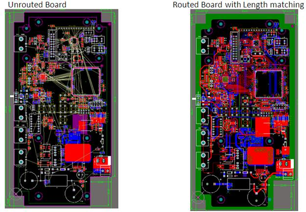
Routing refers to the connecting of the components placed on the board. You can draw vertical traces on one side and horizontal traces on the other which will facilitate wiring of lines crossing over the others. For multiple layers, you need to alternate between directions.
PCB Design verification / PCB DFM:
Implement design rules followed by a check and verification. You need to run DRC from time to time before finally generating CAM files! Complete a design rule check to ensure that all the design rules have been followed during the designing.
Gerber file and NC file o/p:
While generating CAM files you need to make sure that:
Finalize data package for fabrication:
While preparing Data package for fabrication following points must be taken care of:
– PCB Layout data
All copper layer
Solder mask files for outer layers if required
Silk-screen file for top and bottom layer if required
Board outline
Peelable solder mask, Carbon pad layers, etc. if required
– NC drill data
– Fabrication drawing or Mechanical drawing

