


Why is Thickness So Crucial for Printed Circuit Boards?
Designers determine the thickness of a printed circuit board based mainly on its application. During circuit board fabrication, manufacturing processes maintain the specified thickness. As the required thickness depends on the application and functionality of the board, its thickness may vary from design to design. Circuit board fabrication involves several manufacturing processes, and their methods of attaining the final thickness of a printed circuit board may vary, including the tolerance levels. The thickness of a printed circuit board is important because of three factors:
- Cost
- Performance
- Quality
Cost
A major part of the quotation of a printed circuit board consists of the cost of material. If the customer is consistently receiving boards with thickness more than they have stated in the specification and tolerance, the fabricator is using excess material than they are receiving payment for—it is a loss to the fabricator. Conversely, if the customer is consistently receiving thinner boards against their specification and tolerance, they are paying the fabricator more than the agreed price. The cost of material deviating from the specified tolerances may not be very high for a single board or for prototypes. However, for production runs of large scale, the value of material involved may be significant.
Performance
Use of a thinner printed circuit board in place of a thicker one, may cause severe performance degradation. A thinner PCB may develop cracks when subjected to vibrations in the application. On the other hand, a thick board may not fit properly in a slim device, leading to assembly and performance issues.
Quality
Line quality inspection at the manufacturer may reject a printed circuit board deviating from the thickness in the specifications. Customers may also reject such PCBs during their incoming quality inspections.
Thickness Analysis of Printed Circuit Boards
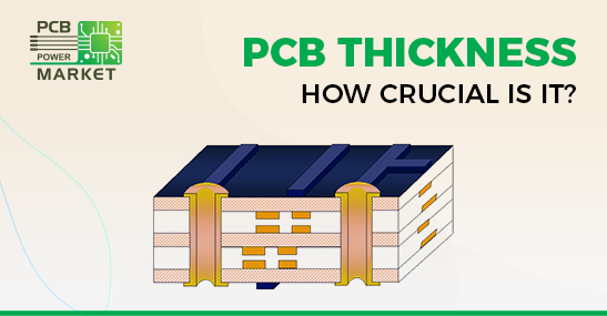
Simple printed circuit boards, whether single- or double-layer, are typically built around a single core or copper clad. For multi-layer boards, it is possible to consider the core of a double-layer board with several layers of pre-preg and copper foil stacked symmetrically around it. More complicated boards may have many cores.
Therefore, the cumulative thickness of the cores together with the individual thickness of all the layers make up the final thickness of a board. An industrial PCB has a standard thickness of 1.57 mm (63 mil). However, thicknesses may range from 0.2 mm to 6 mm.
Although the core, layers of pre-preg and copper foils make up the major part of the PCB thickness, the outermost surfaces of a printed circuit board may also have a solder mask layer and a silkscreen layer adding to the board’s thickness. For instance, a 1.57 mm (63 mil) thick double-layer PCB may have a core of 1.5 mm (59 mil), two copper layers of 0.035 mm (1.38 mil) each, two solder mask layers of 0.01 mm (0.394 mil) each, and one or two silkscreen layers of 0.006 mm (0.226 mil) each.
Manufacturers of modern printed circuit boards offer standard thicknesses depending on the number of layers in the PCB. For instance, a four-layer PCB can have a typical standard thickness of 0.8 mm ±10% and a six-layer board can have a standard thickness of 0.8 mm ±10% or 1.6 mm ±10%. Likewise, an eight-layer board can have a standard thickness of 1.6 mm, 2.4 mm, or 3.2 mm ±10%.
Printed Circuit Board Core Thickness
The core or substrate of a printed circuit board usually consists of epoxy fiber glass with copper foil bonded on both sides. Cores with various thicknesses are available, along with different thicknesses of copper foils. A PCB gets its rigidity from its substrate.
As circuit complexity increases, designers need multiple layers to interconnect the large number of SMDs on the board. As a result, fabricators had to increase the standard PCB thickness from 1.6 mm to 2.4 mm. To comply with RoHS and WEEE requirements, PCB fabricators must use high-temperature substrate materials such as 370HR from Isola in thicknesses of 0.2, 0.3, 0.4, 0.6, and 1.0 mm in multiple layers.
Printed Circuit Board Prepreg Thickness
Manufacturers impregnate prepregs of fiber-weaves with a bonding agent resin. Fabricators use such prepregs for bonding etched cores. For this, they use heat and pressure, thereby varying the thickness of the prepreg layers and adjusting them to the final thickness of the board.
Printed Circuit Board Copper Layer Thickness
Depending on the current handling requirement of the board, its copper layer thickness may vary from 0.036 mm to 0.07 mm. Usually, fabricators use the same copper thickness on both sides of the core layer to prevent the board from curving with heat when undergoing assembly.
Why Thickness is a Crucial Choice?
Although most designers prefer to use standard thickness for their boards, some may need to customize board thickness depending on the specific application. In the final stages of the design, the choice of board thickness impacts several factors. Some of these are:
Weight: The thicker the board, the heavier it will be. For a lightweight device, the designer must look for materials that will result in a thin and light PCB.
Flexibility: Many modern devices need a flexible PCB. As thick boards are usually not flexible, the designer may have to consider thin flexible boards instead.
Space Constraint: With growing demands for slim devices, space is always a constraint. Designers must use low-height components on a thin board.
Components and Connectors: Heavy components will require a thick board to hold them without it bending or sagging. A thin board will support only small and tiny components. For large multi-pin components such as BGAs, designers must pay special attention to the board thickness.
Impedance: A specific dielectric material making up the pre-preg will offer a certain impedance with its thickness. If the designer must change the thickness while retaining the impedance, they must use a dielectric of some other material.
Conclusion
Particular application of a printed circuit board requires specific thickness for its proper functioning. The thickness defines the board’s mechanical rigidity, its signal integrity, and the current carrying capacity of its copper traces. Most designers and PCB fabricators follow IPC guidelines and standards when specifying board thickness and its tolerance for specific applications.

