


Printed Circuit Board Layers
Even the simplest of Printed Circuit Boards or PCBs has many layers. The name printed circuit board implies the designer has printed the circuit on the board for connecting electronic components. Therefore, a PCB will typically have at least four types of layers:
- A Substrate layer
- A Copper layer
- A Soldermask layer
- A Silkscreen layer
Each of the layers above has its own functionality.
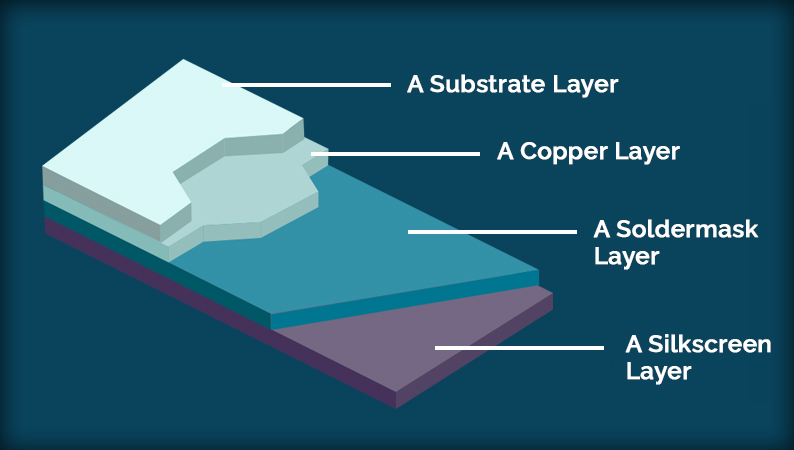
Layer Functionality
- Substrate: A substrate layer provides strength to the PCB. This layer gives the PCB its rigidity, and forms a stable platform on which to position the electronic components. The constituents of a substrate layer are epoxy resin and woven fiberglass cloth, which together form a thin but strong base layer. The commercial name for this combination is FR4, signifying the Fire-Retardant type 4 properties of the material.
- Copper: Manufacturers usually bond a copper layer on to the substrate. Together, this combination becomes a copper clad substrate, or simply a copper clad. A PCB fabricator will remove unwanted copper according to the circuit they have to transfer, and the copper traces remaining on the board act as connections between different electronic components soldered on to specific positions on the board.
- Soldermask: If there is no covering on the copper traces, they will gradually oxidize and become electrically open, and the PCB will stop functioning. Therefore, fabricators use a soldermask layer to cover all copper traces except pads where the components will solder. The soldermask effectively protects the copper traces from exposure to air and thereby increases the life of the board. The soldermask is a thin epoxy layer generally with a green color, although manufacturers may use other colors as well.
- Silkscreen: When there are several components on the board, it is customary to identify their placement by indicating their reference numbers as in the BOM. This is the function of the silkscreen layer. Along with the reference numbers, the silkscreen layer also shows component polarity and other important mounting instructions. Fabricators use white epoxy ink to transfer the information in the silkscreen layer to the PCB.
Layer Quality
The quality of the printed circuit board depends on the quality of its individual layers. Depending on the epoxy type, the substrate has a specific glass transition temperature. If the board temperature crosses its glass transition temperature, the board starts to lose its rigidity and may become deformed. Therefore, it is very important to use a substrate with a glass transition temperature that is higher than the temperature of the application.
The etching process defines the quality of the copper traces. The weight of copper of the copper clad defines the thickness of the copper trace, but the etching process defines its width. Over-etching may reduce the width of the trace, increasing its resistance. If the trace must carry a large amount of current, increased resistance may raise the temperature of the track high enough to melt it. Under-etching may make the width of the trace more than the specifications, thereby increasing the chances of an electrical short with a neighboring trace during soldering.
The quality of the soldermask depends on the registration and thickness of the mask. It is important that the registration of the soldermask with the circuit on the board is highly accurate, especially for fine pitch components. Unless the soldermask finger between two close pads is in proper position, there is a possibility of dry solder on some pads. The thickness of the mask must be uniform across the board to prevent unwanted peeling off in the areas where the mask is thin.
It is very important that the silkscreen layer has legible characters and sharply defined lines to be of high quality. The assembly operator must be able to place the components in their specified positions for the board to function properly.

Get Instant Quote
Multi-Layer Boards
A printed circuit board may be of single-layer, double-layer, or multi-layer types. While a single layer board has a single copper clad substrate, a double-layer board will have a substrate with a copper layer on both sides. It is usual to consider a multi-layered board as a double-layered board with additional copper layers on both sides, separated by prepreg or insulating layers. Fabricators usually distribute the additional copper layers equally on both sides of the central substrate.
The number of layers or the stack build-up of the PCB depends on the circuit complexity and the overall size of the board. To enable proper routing of all nets after proper positioning of the components, the designer must use several copper layers. However, the solder mask and silkscreen layers appear only on the two outermost copper layers. To reduce the number of copper layers, the customer has the option of increasing the size of the board, or of reducing the number of components on the board.
PCB Materials
- FR4: Glass epoxy FR4 is one of the most popular as a substrate material. This is because FR4 remains stable even when exposed to heat up to a temperature of 130oC. Only beyond this temperature, it starts to lose its solid form or rigidity and its electrical insulation properties.
- Hylam: Designers select the substrate material depending on the ambient temperature of the application. They must select a substrate with a glass transition temperature above that of the maximum temperature the application is likely to experience. If the application temperature is low, designers may use cheaper material for the substrate. One of such materials is Hylam or Bakelite Hylam.
Hylam has good rigidity and insulation properties. However, unlike glass epoxy, hylam does not exhibit fire retardant properties. That means, if hylam catches fire, it continues to burn, whereas for glass epoxy the fire does not burn very long. This is one major reason hylam is not reliable for use as a substrate material. - Copper: Copper is the most popular material for use on the printed circuit board for connecting components. There are several reasons for this. Copper has:
- High Electrical Conductivity — copper traces have low resistance
- High Mechanical Ductility — copper can spread in thin sheets on the substrate
- High Melting Point — copper traces can carry higher current without melting
- High Availability — reasonable cost of PCB fabrication
- Prepreg: Multi-layered boards use prepregs as insulators to glue the substrates and different layers of copper. The prepreg or pre-impregnated layer is the material that holds the entire board together. Fabricators make prepreg of fiberglass impregnated with epoxy resin. They press the layers together at a high temperature to build up the board thickness.
- Aluminum Boards: Some boards, especially those meant for mounting high-power LED lights, use a backing of an aluminum sheet. These are metal-clad boards and the aluminum backing is for dissipating the heat that the LED chips generate when operating.
Frequently asked questions
Q1. What are the main layers of a printed circuit board?
A standard printed circuit board typically consists of a substrate layer, copper layer, solder mask layer, and silkscreen layer. Each layer serves a specific mechanical, electrical, or assembly-related function.
Q2. What is the purpose of the substrate layer in a PCB?
The substrate provides the mechanical strength and rigidity of the PCB while acting as an insulating base for the copper circuitry.
Q3. What is the difference between a single-layer PCB and a multilayer PCB?
A single-layer PCB contains one copper layer, while a multilayer PCB contains multiple copper layers separated by insulating prepreg materials to support more complex circuit designs.
Q4. Why is FR4 commonly used in PCB manufacturing?
FR4 offers a combination of mechanical strength, electrical insulation, flame-retardant properties, and cost-effectiveness, making it one of the most widely used PCB substrate materials.
Q5. How can I get an instant quote for PCB fabrication and assembly?
You can upload your PCB design files through PCB Power's online platform to receive an instant quote for PCB fabrication and assembly.

